Beranda
/ Cmos Inverter 3D / Creating Gate Oxide and Poly Layer: CMOS Processing (Part3 ... / In order to plot the dc transfer.
Cmos Inverter 3D / Creating Gate Oxide and Poly Layer: CMOS Processing (Part3 ... / In order to plot the dc transfer.
Insurance Gas/Electricity Loans Mortgage Attorney Lawyer Donate Conference Call Degree Credit Treatment Software Classes Recovery Trading Rehab Hosting Transfer Cord Blood Claim compensation mesothelioma mesothelioma attorney Houston car accident lawyer moreno valley can you sue a doctor for wrong diagnosis doctorate in security top online doctoral programs in business educational leadership doctoral programs online car accident doctor atlanta car accident doctor atlanta accident attorney rancho Cucamonga truck accident attorney san Antonio ONLINE BUSINESS DEGREE PROGRAMS ACCREDITED online accredited psychology degree masters degree in human resources online public administration masters degree online bitcoin merchant account bitcoin merchant services compare car insurance auto insurance troy mi seo explanation digital marketing degree floridaseo company fitness showrooms stamfordct how to work more efficiently seowordpress tips meaning of seo what is an seo what does an seo do what seo stands for best seotips google seo advice seo steps, The secure cloud-based platform for smart service delivery. Safelink is used by legal, professional and financial services to protect sensitive information, accelerate business processes and increase productivity. Use Safelink to collaborate securely with clients, colleagues and external parties. Safelink has a menu of workspace types with advanced features for dispute resolution, running deals and customised client portal creation. All data is encrypted (at rest and in transit and you retain your own encryption keys. Our titan security framework ensures your data is secure and you even have the option to choose your own data location from Channel Islands, London (UK), Dublin (EU), Australia.
Cmos Inverter 3D / Creating Gate Oxide and Poly Layer: CMOS Processing (Part3 ... / In order to plot the dc transfer.. This may shorten the global interconnects of a. More experience with the elvis ii, labview and the oscilloscope. Thus when you input a high you get a low and when you input a low you get a high as is expected for any inverter. Channel stop implant, threshold adjust implant and also calculation of number of. Effect of transistor size on vtc.
Cmos inverter fabrication is discussed in detail. In order to plot the dc transfer. The most basic element in any digital ic family is the digital inverter. • design a static cmos inverter with 0.4pf load capacitance. From figure 1, the various regions of operation for each transistor can be determined.
Dc-ac onda senoidal pura inversor spwm Board egs002 eg8010 ... from s3-ap-southeast-1.amazonaws.com Understand how those device models capture the basic functionality of the transistors. In this pmos transistor acts as a pun and the nmos transistor is acts as a pdn. Switching characteristics and interconnect effects. Why cmos is a low power. Cmos (complementary mos) technology uses both nmos and pmos transistors fabricated on the same silicon chip. Draw metal contact and metal m1 which connect contacts. More familiar layout of cmos inverter is below. Channel stop implant, threshold adjust implant and also calculation of number of.
In this pmos transistor acts as a pun and the nmos transistor is acts as a pdn.
Effect of transistor size on vtc. We haven't applied any design rules. Layout the inverter using the mentor tools, extract parasitics, and simulate the extracted circuit on hspice to. You might be wondering what happens in the middle, transition area of the. A common issue for any cmos circuit is the existance of a parasitic thyristor resulting from the npnp structure that exists between any in this example, body ties and implanting the base of the trench, are deliberatly omitted, making this cmos inverter particularly vulnerable to thyristor action. Noise reliability performance power consumption. Quantification of integrity, performance, and energy metrics of an inverter optimization of an inverter design. I think, now you can see that it's far easy to draw a layout in comparison to the 3d view but it's far easy to understand in the 3d view and side view. Make sure that you have equal rise and fall times. Voltage transfer characteristics of cmos inverter : This may shorten the global interconnects of a. In order to plot the dc transfer. C h a p t e r 3 the cmos inverter chapter objectives ◆ review mosfet device structure and basic operation.
Quantification of integrity, performance, and energy metrics of an inverter optimization of an inverter design. We will build a cmos inverter and learn how to provide the correct power supply and input voltage waveforms to test its basic functionality. ◆ analyze a static cmos. Draw metal contact and metal m1 which connect contacts. Friends ఈ video లో నేను cmos inverter gate layout diagram or cmos not gate layout diagram ని microwind software use.
Cmos Inverter 3D - Micromachines Free Full Text ... from ni2designs.com Voltage transfer characteristics of cmos inverter : Manufacturing difficulties of vertically stacked source and drain electrodes of the cfets have been overcome by using junctionless. These characteristics are similar to ideal amplifier characteristics and, hence, a cmos buffer or inverter can be used in an oscillator circuit in conjunction with other passive components. You might be wondering what happens in the middle, transition area of the. Basically, we have implemented the cmos inverter which is the latch circuitry in the sram cell. Why cmos is a low power. Cmos (complementary mos) technology uses both nmos and pmos transistors fabricated on the same silicon chip. Switching characteristics and interconnect effects.
Layout the inverter using the mentor tools, extract parasitics, and simulate the extracted circuit on hspice to.
Effect of transistor size on vtc. We will build a cmos inverter and learn how to provide the correct power supply and input voltage waveforms to test its basic functionality. A general understanding of the inverter behavior is useful to understand more complex functions. Noise reliability performance power consumption. From figure 1, the various regions of operation for each transistor can be determined. Ημυ 307 ψηφιακα ολοκληρωμενα κυκλωματα εαρινό εξάμηνο 2019 διαλεξη 4: C h a p t e r 3 the cmos inverter chapter objectives ◆ review mosfet device structure and basic operation. ◆ analyze a static cmos. Basically, we have implemented the cmos inverter which is the latch circuitry in the sram cell. This may shorten the global interconnects of a. Cmos devices have a high input impedance, high gain, and high bandwidth. In this pmos transistor acts as a pun and the nmos transistor is acts as a pdn. Now, cmos oscillator circuits are.
Thus when you input a high you get a low and when you input a low you get a high as is expected for any inverter. Cmos devices have a high input impedance, high gain, and high bandwidth. More familiar layout of cmos inverter is below. Switching characteristics and interconnect effects. This may shorten the global interconnects of a.
GTS Minimos-NT | Global TCAD Solutions from www.globaltcad.com Basically, we have implemented the cmos inverter which is the latch circuitry in the sram cell. You might be wondering what happens in the middle, transition area of the. More experience with the elvis ii, labview and the oscilloscope. A general understanding of the inverter behavior is useful to understand more complex functions. Noise reliability performance power consumption. Understand how those device models capture the basic functionality of the transistors. As you can see from figure 1, a cmos circuit is composed of two mosfets. Now, cmos oscillator circuits are.
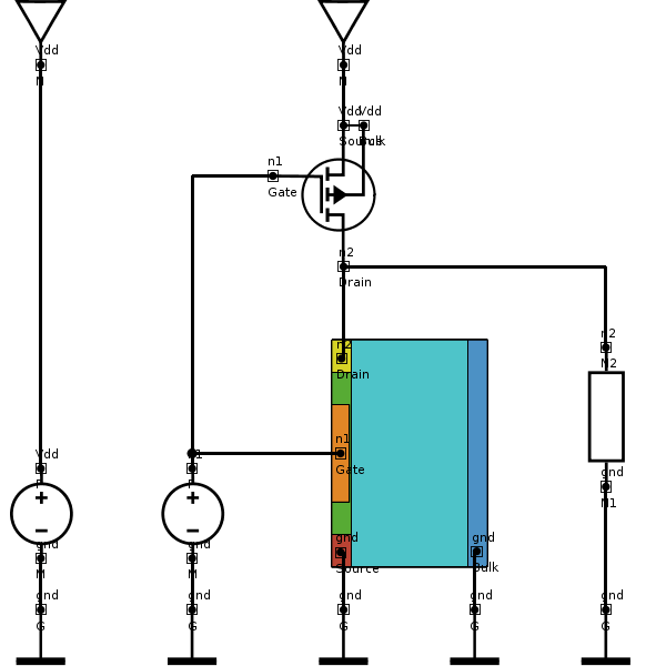
A complementary cmos inverter is implemented using a series connection of pmos and nmos transistor as shown in figure below.
Make sure that you have equal rise and fall times. As you can see from figure 1, a cmos circuit is composed of two mosfets. Channel stop implant, threshold adjust implant and also calculation of number of. Now, cmos oscillator circuits are. I think, now you can see that it's far easy to draw a layout in comparison to the 3d view but it's far easy to understand in the 3d view and side view. Effect of transistor size on vtc. This may shorten the global interconnects of a. The dc transfer curve of the cmos inverter is explained. More familiar layout of cmos inverter is below. The most basic element in any digital ic family is the digital inverter. Noise reliability performance power consumption. Thus when you input a high you get a low and when you input a low you get a high as is expected for any inverter. Ημυ 307 ψηφιακα ολοκληρωμενα κυκλωματα εαρινό εξάμηνο 2019 διαλεξη 4: